


Description
Special Request:
1. 1-step HDI Blind and Buried Via PCB.
2. Blind via holes made by laser need to be filled
with resin+ copper capped plating of filled via holes.
3. Impedance Control.
Layer: 4L
Base Material: FR4 IT150GTC, PP: IT-150GBS
Board Thickness: Non-antenna Area: 0.5+/-0.1mm;
Antenna Area: 0.428+/-0.1mm
Outer Layer Final Copper Thickness: 30um
Inner Layer Final Copper Thickness: 25um
Base Copper Thickness: 1/3OZ
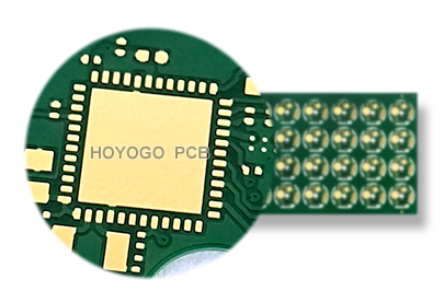
Surface Finished: ENIG
Unit Size(mm): 28.63*30.40
Min. W/S(mil): 3.94/3.94
Min. Hole Size: 0.1mm