


2022-11-30 14:56:00
Electronic products and equipment used in our daily life, as long as there are electronic components such as integrated circuits, there is the existence of PCB. In PCB processing, due to the differences in technical requirements and manufacturing capabilities, there are many special technologies with high technical threshold, high cost and long cycle. So what are the relatively special PCB technologies?
1. Impedance Control
When digital signals are transmitted on a PCB, the characteristic impedance value of the PCB must match the electrical impedance of the head and tail components. Once mismatched, the transmitted signal energy will be reflected, scattered, attenuated or delayed. In this case, impedance control must be performed to match the characteristic impedance value of the PCB to the component.
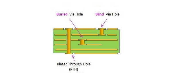
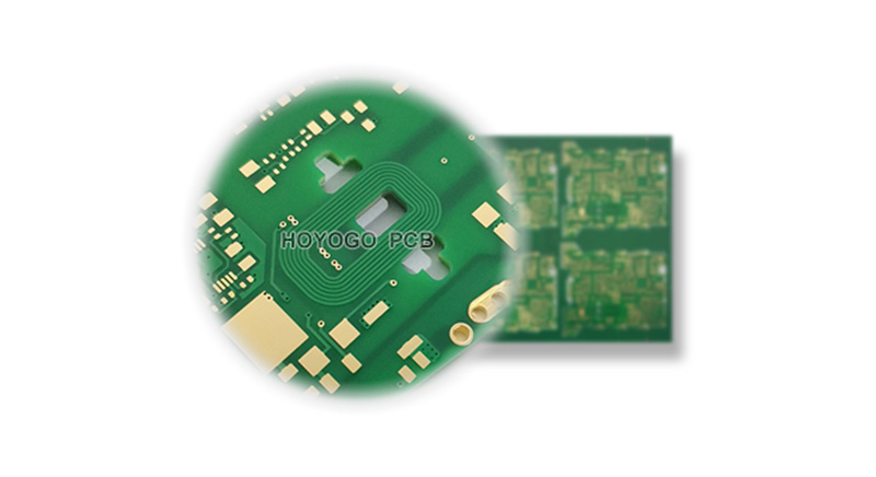
2. Blind and Buried Via
Blind Via: It is a hole in one of the top or bottom layers, but cannot be seen through. Buried Via: It is on the inner layer of the PCB, the surface is invisible. The application of blind & buried vias can greatly increase the available space of the circuit layers and enable interconnection between any layers within the circuit board.
3. Heavy Copper PCB
When the thickness of the copper foil of the CCL is greater than or equal to 2OZ, it is defined as a thick copper PCB. Compared with ordinary circuit boards, heavy copper PCB can carry larger currents. When passing a large current, the temperature rise is small, and it has better heat dissipation.

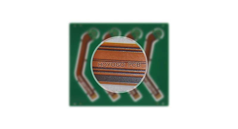
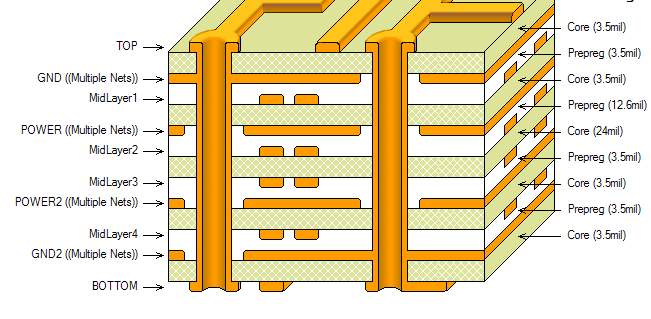
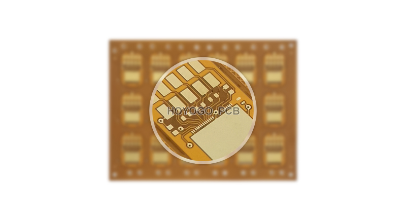
4. Multi-layer Special Laminated Structure
Laminated structure is a major factor affecting PCB EMC performance and a method to suppressing electromagnetic interference. For a design with a large number of signals, high device density, and high signal frequency, a multilayer special stack structure is usually used.
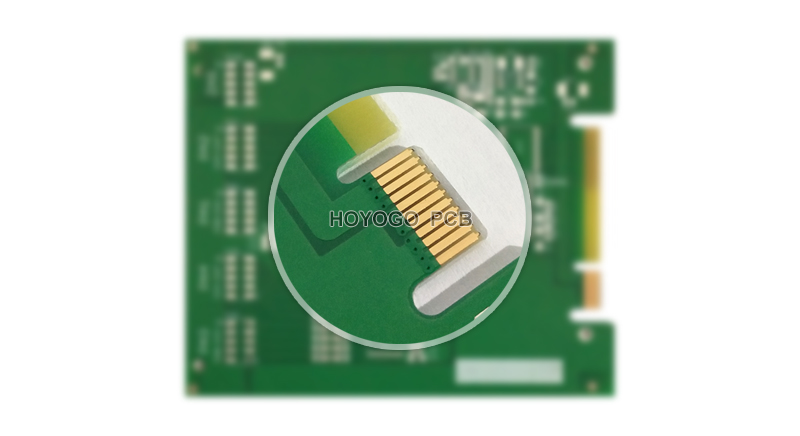
5. Electroplated nickel gold
Nickel-gold electroplating means that gold particles are attached to the PCB by electroplating. Because of the strong adhesion, it is called hard gold. Using this process, the hardness and wear resistance of the PCB can be greatly increased, the diffusion of copper and other metals can be effectively prevented, and the plating layer is uniform and fine, which is usually used on gold fingers.
6. ENEPIG
ENEPIG is a surface treatment process by chemically depositing a layer of nickel, palladium and gold on the surface of the PCB during PCB processing. It can make the PCB have good conductivity, corrosion resistance and friction resistance.
7. Irregularly-shaped Hole
The production of non-circular holes in PCB processing is called special irregularly-shaped holes. These holes include figure-8 holes, diamond-shaped holes, square holes, sawtooth-shaped holes, etc. There are also two types of copper in the hole(PTH) and no copper in the hole(NPTH).
8. Depth Control Slots
With the development of the diversification of electronic products, special concave fixed components are gradually applied to the PCB, resulting in the formation of depth control slots.
HoYoGo is an international, professional and reliable PCB manufacturer. HoYoGo, hit your goal on PCB. We have profound engineering and technical capabilities, flexible supply chain management capabilities, excellent quality levels, and strong production capabilities. If you have PCB production needs, please contact us.