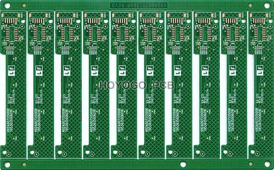

With the continuous development of the electronics industry, there are more and more PCB surface treatment technologies, and each technology has its own merits. OSP is a commonly used surface treatment technology process, what are its advantages and disadvantages?

Compared with other surface treatment technologies, OSP is somewhat different. It uses a chemical method to produce an organic film on the clean bare copper surface, which acts as a barrier between the copper and the air. OSP is organic, not metallic, and its cost is lower than most surface treatment technologies.
Advantages:
With this organic film, it can resist the attack of moisture in the air without being oxidized before welding, can withstand the test of high temperature, maintain good activity, and has a good tinning ability. This layer of organic film will not cause damage to the sheet material. It can be easily removed by the solder resist during soldering. It can solder the copper wire and the components together in a very short time, and there will be no organic film remaining on the board.
Disadvantages:
The protective film formed by the OSP technology is extremely thin and easily scratched, requiring careful operation and operational amplifier. It is also necessary to avoid printing errors as much as possible, because cleaning will damage the OSP protective layer.
Each surface treatment technology process has advantages and disadvantages, and different technologies are used in different occasions. At present, there is no perfect PCB surface treatment technology that can meet all PCB application scenarios. HOYOGO is an international, professional and reliable PCB manufacturer. Our production strictly follows the high-quality system, all products strictly follow the acceptance standards IPC-A-600-H and IPC-6012, and we can guarantee the quality and reliability of each product delivered to our customers.
