


2020-01-08 17:02:54
Printed circuit boards have been the provider of electrical connections for electronic components for more than 100 years. Since the development of the PCB manufacturing industry, it has reached a rather sophisticated level, and many improved and optimized circuit board technologies have also been born. This article mainly outlines the key technologies for producing high-density interconnect circuit boards, high-density arbitrary-layer interconnect circuit boards, and integrated printed circuit boards.
1. High-Density Interconnect Circuit Boards
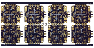
In the early 1990s, Japan and the United States pioneered the application of High Density Interconnect Technology (HDI). Its manufacturing process is to use double-sided or multi-layer boards as the core board, and use multi-layer overlapping stacking technology to maintain a PCB with absolute insulation between each layer of the layout, to manufacture high-density, highly integrated electronic circuit boards. The five characteristics of this type of PCB are "mini, thin, high frequency, fine, and heat disspation.” According to these five characteristics, continuous technological innovation is the development trend of today’s high-density electronic circuit boards. “Thinning” determines the survival basis of high-density electronic circuits. Its birthday directly caused and influenced the prodcution of fine, miniature technology. The design of the connection wires, fine micro-drilled holes and the insulation of each layer determines whether the high-density electronic circuit board can adapt to high-frequency work and whether it is conducive to reasonable heat conduction. This is also an important method for judging the degree of integration of electronic circuits in ultra-high-density electronic circuit boards.
2. High-density Arbitrary-layer Interconnect Circuit Boards

For HDI of different hierarchies, there are large differences in technology process manufacturing. Generally, the more multi-layered structures, the more complex and precise, the more difficult it is to manufacture. At present, there are several major process characteristics in the way of associating the layers, which are “step connection”, “wrong hole connection”, “cross-layer connection” and “stacked hold connection”, which will not be repeated here. Ultra-high-density arbitrary-layer interconnect PCB, which belongs to high-end products in PCB. Its biggest demand comes from the electronic product markets that requires light, thin and versatile features, such as smartphones, laptops, digital cameras and LCD TVs.
3. Integrated Printed Circuit Boards
Integrated printed circuit board technology is to integrate one or more separate electronic components (such as resistors, capacitors, capacitors, etc.) into a printed circuit board structure. It has the advantages of making the integrated PCB have a certain degree of system functions, improving the reliability of electronic product system functions, improving signal transmission performance, effectively reducing production costs, and making the production processes more environmentally friendly. Integrated PCB technology is also a technical approach to the integration and miniaturization of electronic device systems, which has huge market development potential. The system integration technology of embedded electronic components in PCB has begun to enter the foreigh application stage, and has made breakthroughs in related materials and manufacturing process technologies, and industry-leading foreign companies have begun to put the technology into mass production.
With the development of electronic technology, PCB manufacturing will have more improvements and innovations in the future. They not only have excellent usability, but also have a lower damage rate and a longer service life than ordinary PCBs.