


2022-12-08 16:55:44
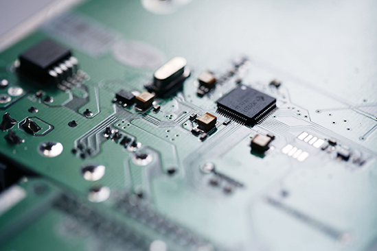
Vias are one of the important components of a PCB. A via is mainly composed of two parts, one is the drill hole in the middle, and other is the pad area around the drill hole. In the PCB manufacturing process, there are 3 methods of processing vias. What are these?
1. Vias covered with solder mask ink
Vias covered with solder mask ink means that the solder ring of the via is not exposed and covered with solder mask ink, which not only ensures the electrical performance, but also avoids the risk of short circuit with other components during use.
2. Vias with solder mask opening
Vias with solder mask opening means that the solder ring of the via is exposed and not covered with solder mask ink. This processing method is similar to the processing method for plug-in holes. The plug-in holes generally require opened and tinned. This kind of processing is usually carried out when there are special needs for vias with solder mask opening. If the surface treatment is HASL, the vias treated in this way can be tinned and soldered like the patch pads.
3. Plug Via with Solder Mask
Plug Via with Solder Mask refers to plugging the entire via with solder mask ink. The best standard for plug via with solder mask is that via hole is opaque, that is, it cannot be seen through from one side of the hole to the other side.
To sum up, the 3 processing methods of PCB vias have their own characteristics, and you can choose the appropriate via processing method according to your own product attributes.
HoYoGo is an international, professional and reliable PCB manufacturer. The management team has average of 25 years of industry experience. We also have 2 factory production bases with a monthly production capacity of 500,000 square meters. Relying on our rich experience, production capacity and resources, we can provide you with one-stop service for mass production from small to large.